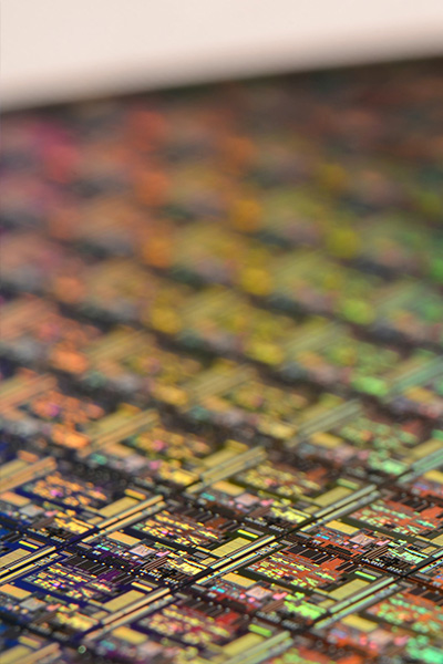
Following of geometric, structural, optical and electrical properties of structures and materials
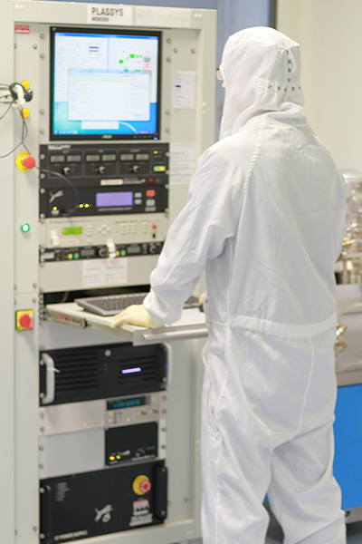
The laboratory provides control of the complete set of integrated circuit parameters (geometric, structural, optical, electrical) parameters throughout the entire cycle of their creation, starting with the development of the initial structure creation technology and ending with the research of the ready-made integrated circuits. Methods of operational control of reliability in the production of integrated circuits based on CVD structures have been developed and implemented on laboratory equipment. The laboratory is ready to provide services for conducting analytical studies on existing equipment
Monitoring geometric parameters
Contact profilometry
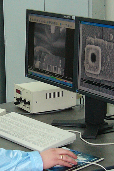
Optical and scanning electron microscopy
Photometry and ellipsometry
Optical and scanning electron microscopy
Photometry and ellipsometry
Monitoring OF THE RESISTIVITY OF MATERIALS BY THE FOUR-PROBE METHOD
Monitoring OF ELECTROPHYSICAL PROPERTIES OF ELEMENTS AND TEST STRUCTURES
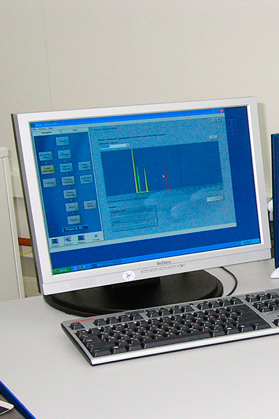
Monitoring impurity composition
Secondary ion mass spectrometry
X-ray fluorescence spectroscopy
Energy dispersion spectroscopy
X-ray fluorescence spectroscopy
Energy dispersion spectroscopy
Related Services

Automated measurements of surface resistance
- Measuring range 5mΩ/cm ÷ 5mΩ/cm;
- Measurement accuracy < 0,5 %;
- Working plate diameter up to 200 mm;
- Edge exclusion up to 3 mm;
- Ability to work with rectangular-square samples when manually loading samples
Control of linear dimensions of topology and cross-section elements
- Resolution:
– in secondary electrons, not more than 1 nm
– in the reflected electrons, not more than 3 nm
– in passed electrons, not more than 1 nm - Magnification adjustment range, 20 - 1000000 x
- Measuring range of linear dimensions, 0.02 - 5000 µm
- Limits of permissible error when measuring linear dimensions:
– in the range from 0.02 µm to 0.2 µm no more than 10 nm
– in the range from 0.2 µm to 0.8 µm no more than 40 nm
– in the range from 0.8 µm to 5000 µm no more than 4%
Surface Relief Modification
- Resolution:
- surface (lateral), 10 nm,
- in depth, 10 nm - Range of linear dimensions of processed primitives 0,05 ÷ 100 µm
- The accuracy of the location of the primitives is not worse, 100 nm
- Accelerating voltage adjustment range, 0,5 ÷ 30 kV
- Materials used for Ga, Pt, C, SiO2 processing
Material Surface Profile Control
- Maximum scanning length 200 mm;
- Maximum scan area: any rectangle inscribed in a circle with a diameter of 200mm;
- Lateral resolution X=25 nm, Y=1 µm;
- Vertical range:
±3,25 µm, resolution < 1 Ǻ;
±13 µm, resolution < 2 Ǻ;
131 µm, resolution < 8 Ǻ Maximum scan area: any rectangle inscribed in a circle with a diameter of 200mm
- Vertical Accuracy ± 0.1% of upper range;
- Reproducibility 7.5 Ǻ or 0.1% (1σ);
- Repeatability 15 Ǻ or 0.25% (1σ), whichever is greater;
Monitoring of electrical parameters
- Voltage range from 2µV to 100V;
- Current range from 1fA to 1A;
- Signal frequency when measuring from 20Hz to 2MHz;
- Resistance range from 1×10-18 to 999,9999×10¹⁸ Ohm;
- Vertical Accuracy ± 0.1% of upper range;
- Reproducibility 7.5 Ǻ or 0.1% (1σ);
- Repeatability 15 Ǻ or 0.25% (1σ), whichever is greater

Appearance control
- Resolution in the visible range 0.5 µm;
- Resolution in UV light 0.1 µm;
- Permissible absolute error range ±0.03 µm;
- Zoom range, 50 ÷ 1500

Measurements of the thicknesses of multilayer thin-film structures and their optical characteristics
- Wavelength range 265 nm ÷ 1700 nm;
- Range of measured thicknesses 1 Å-100 µm;
- Limiting accuracy of thickness measurement (1σ) 0.25Å
Statement of technological processes for the manufacture of wafers with microchip crystals
- SOI CMOS, design standards 0.35 µm, number of metallization levels 4, supply voltage 3.3V;
- CMOS on bulk silicon, design standards 1.6 µm, number of metallization levels 1 and 2, supply voltage 12V and 16V;
- CMOS on KNS-0.3/0.6, design standards 1.6 µm, number of metallization levels 1 and 2, supply voltage 5V, 7V and 36V;
- KNS-5, design standards 1.6 µm, number of metallization levels 1 and 2, supply voltage 3V
Qualitative-quantitative elemental analysis
- Accelerating voltage adjustment range 0,2 kV ÷ 30 kV;
- The range of elements recorded using an X-ray energy-dispersive spectrometer from 5V to 92U;
- Limits of permissible relative error in measurements of the mass fraction of elements in the range from 6С to 92U in samples no more than:
– for elements with a mass fraction range of more than 10% ±4%
– for elements with mass fraction range from 1% to 10% ±20%
– for elements with mass fraction range from 0,1% to 1% ±50%